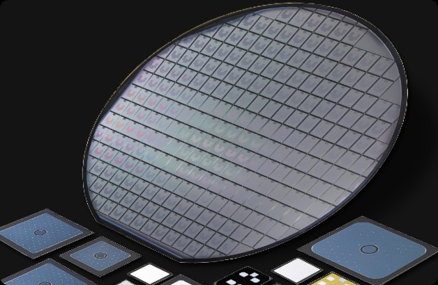
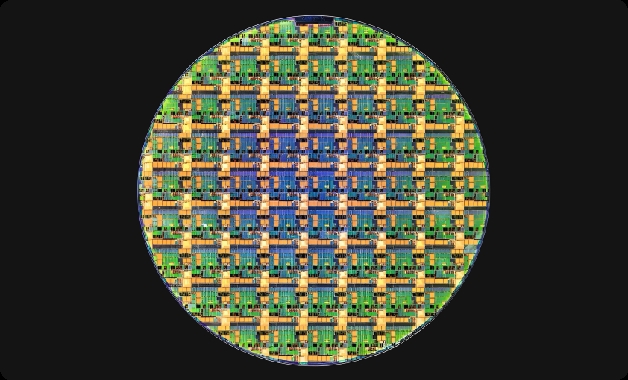
Wafer appearance defect detection
Application background
Wafer inspection is a constantly evolving field that involves many advanced technologies and algorithms. The surface of wafers is usually very small and requires high-precision image acquisition and processing. Through continuous research, innovation and development of related technologies are promoted
Detection range
Foreign objects, scratches, bubbles, pockmarks, dirt, ink stains, etc
Detection effect
Can improve detection efficiency and save a lot of manpower and time costs